test
The term test in this context refers exclusively to the testing of electronic components, assembled printed circuit boards and assemblies, as well as to the test procedures used for this purpose. Tests are designed to detect malfunctions, optimize manufacturing, improve manufacturing quality, increase manufacturing yield, and reduce the costs that defective components cause. Tests are integral parts of electronic manufacturing, and their results directly affect manufacturing processes.
Test procedures are divided into built-in self-tests, structural tests and functional tests, as well as optical and electrical test procedures and the stress tests, the burn-in tests.
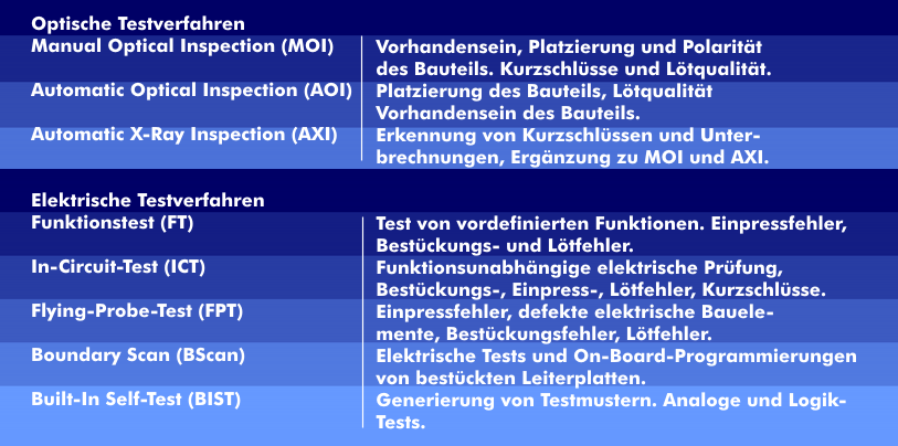
The optical test procedures consist of the manual visual inspection, Manual Optical Inspection(MOI), the automatic optical inspection, Automatic Optical Inspection ( AOI), and the automatic X-ray inspection, Automatic X-ray Inspection( AXI).
In addition to the classic electrical test methods such as the Functional Test( FT), Flying Probe Test ( FPT) and In-Circuit Test( ICT), further functional and optical test methods have been added. These include the boundary-scan test( BST), the optical AOI test and the AXI test, which uses X-rays.
Due to increasing miniaturization, assembled modules can only be tested to a limited extent and at great expense using conventional electrical test methods. In addition, the connections of certain packages are located below the chip and are therefore not accessible at all, as is the case with BGA packages. In order to still be able to meet the high quality requirements, the combination of electrical and optical test methods is recommended.
Defect detection and the combination of test methods
All test methods have certain advantages that become apparent in the detection of manufacturing defects. With the sensible combination of several test procedures, an almost complete defect detection is possible. Optimum test coverage is provided by the combination of visual inspection (MOI), automatic optical inspection (AOI) and flying probe testing (FPT). Some of these tests can also be used if the chip connections are not accessible, as in the case of the BGA package or the SOJ package.
Testable defects can be classified as placement defects, solder defects, and component defects. Assembly errors include the presence or absence of the correct component, placement, and correct location corresponding to polarity. Soldering defects include breaks and shorts in traces, as well as solder quality, which can be affected by cold solder joints, missing or excessive solder. And component faults involve the correct component values of resistors, coils, capacitors and chips, as well as functional faults of complex components.
In general, the goal is to detect and correct defects as early as possible, thereby reducing costs and optimizing the manufacturing process.