package
In electronics, a package is the constructive housing design of an integrated circuit. In the case of transistors, this is referred to as the transistor package. Package development is directly linked to chip development. In order to meet the increasing demands on functionality, space requirements, the rapidly increasing number of connections and processing technology, new package designs for analog and digital chips have been and are constantly being developed, which differ in their compactness, size, flatness and the position and type of connection technology and the pitch for the connection contacts.
A general classification of the packages can be made by the processing technology. According to this, there are packages for through-hole technology( THT) and surface mounted technology( SMT) with surface mounting.
Packages for through-hole technology
Historically, the first chip packages were for through-hole technology. The connections to the package were arranged in a row one behind the other, on one or both sides of the package.
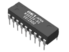
The pins themselves were straight and passed through the holes in the PCBs. The package types were the Single Inline Package( SIP) with one row of contacts and the Dual Inline Package( DIP) with two rows of contacts on the long sides of the package. Both designs are still in use. These SIP packages and DIL packages are available in plastic and ceramic, in which case the designation is preceded by the letter "C", for ceramic, as in the case of the Ceramic Dual Inline Package( CDIP), for example. As the number of connections increased, the package was enlarged and the distance between the connections, the pitch, was reduced.
Packages for SMT technology
Parallel to this development, packages for SMT technology appeared. In these packages, the connection pins are not straight, but angled outwards or under the package.
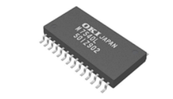
Again, the division into plastic and ceramic construction. As far as the plastic design is concerned, there are packages with contact rows on both sides and connections angled outwards. These include the Small Outline Package( SOP), Thin Small Outline Packages( TSOP), Thin Shrink Small Outline Packages( TSSOP) and Very Thin Small Outline Packages (VTSOP).
The situation is different for the J-connectors, which are angled under the chip package as in the SOJ package. The pin density was reduced and because of the increasing number of pins, the pins were on all four package sides resulting in the quad packages such as the Quad Flat Package( QFP). In this technology, the distances between the connections were also reduced and bent under the package to save space.
The miniaturization of packages
The next stage in the development of packaging was ball grid packages, in which the connections are located as contacts on the underside of the package. In this technology, central processing units( CPU) are designed with several hundred connections. In addition, the Ball Grid Array( BGA) technique is used in the smallest packages.
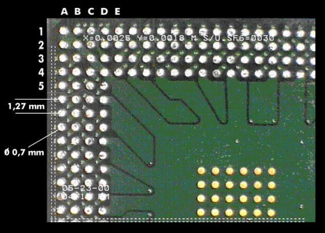
In addition to the number of connections, the development of chip packages is characterized by the continuous reduction of the distances between the connections and the flat design construction. For example, shrink small outline packages( SSOP) have a pin spacing of only 0.4 mm and super-thin leadless leadframe packages( LLP) have a thickness of only 0.4 mm. In the miniaturized BCC( bump chip carrier) and CSP(chip scale package) packages and their variants used in mobile devices, the package is only slightly larger than the actual chip.
Miniaturization has also progressed rapidly in chips with analog technology. DSSP packages include filters with a footprint of half a square millimeter.