3D-NAND (3D-NAND)
NAND flash are non-volatile memories with sequential access. 3D NAND cells are flash memories as 3D ICs in which the planar memory cells are stacked vertically on top of each other. These NANDs are also referred to as V-NANDs or 3D V-NANDs (Vertical).
The stacking technique achieves greater compactness and a better storage capacity-to-volume ratio. Shorter interconnections between memory cells can increase storage capacity and storage speed and reduce power consumption. Memory capacity is increased by multi- level memory cells, Multi Level Cells( MLC), which operate at four voltage levels, Triple Level Cells( TLC), which operate at eight levels, and Quadruple Level Cell( QLC), which know sixteen levels.
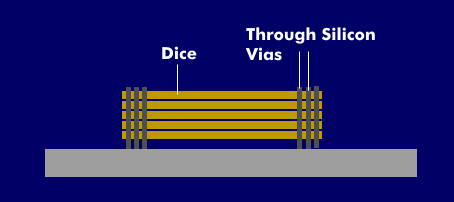
To increase memory speed, 3D NAND technology also relies on different bonding. Instead of wire bonding for each die, it uses a silicon through-silicon via ( TSV) to bond the dice together. A cylindrical channel runs between the vertically stacked memory cells. This technology is referred to as channel hole technology (CHT).
The increase in write speed is achieved by another technology called Charge Trap Flash( CTF), which temporarily stores the electrical charge on a non-conductive layer ofsilicon nitride.
Back in 2014, there were 3D NAND flashes consisting of 24 and 32 stacked layers. A few years later, 3D NANDs with 64 layers were produced. 3D NAND technology makes it possible to develop solid-state drives with storage capacities of 32 terabytes( TB).