through-silicon via (TSV)
Through-Silicon-Via(TSV) technology is a silicon-based through-hole plating technique. TSV technology is used to create the shortest possible connection between the bottom of the chip to the top of the chip.
Through-silicon vias allow the shortest possible connections to be made from the top metallic layer of a chip to the bottom surface. The technique reduces power consumption and achieves higher data rates than wire bonding because of the shorter connections.
-Foto-statschippac-com.png)
TSV technology lends itself to vertically arranged DRAMs and NAND gates, the 3D NANDs, in addition to optoelectronics and microsystems technology( MST) components, where TSV technology is used in the fabrication of vertical interconnects between the integrated subchips of a system-in- package( SiP).
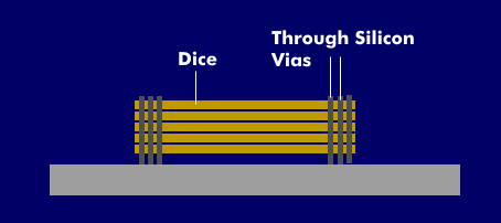
The TSV technique can be used to etch microvias with a diameter of about 30 µm and a depth of several hundred micrometers into semiconductors. These non-conductive junctions are filled with an electrically conductive metal, usually copper.