bonding
In classic chip manufacturing, the chip core, called a die , is attached to a ceramic or plastic substrate. The die itself is only a few millimeters small and has many contacts on the die surface or die undersurface. In addition to the bonding mentioned above, the term bonding is also used for bundling. Thus as line bonding for line bundling in the context of VDSL2.
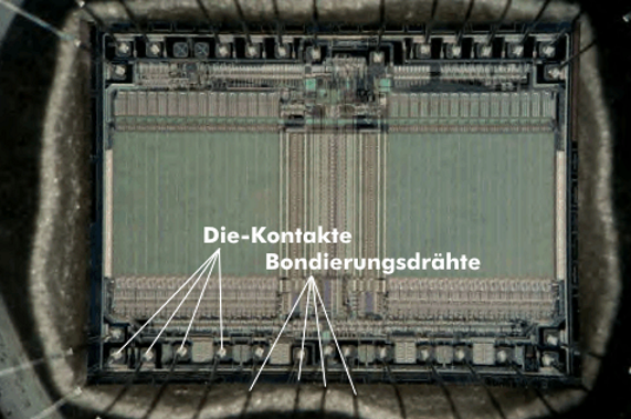
Since the die contacts are not accessible and, moreover, a user could not connect to the die contacts, the die contacts must be connected to the package ports. This process is called bonding or bonding. Wire bonding uses microfine wires to make a connection between the bond pads on the die and the socket terminals. The connection can be made using soldering techniques, ultrasonic welding or bonding methods.
Bonding techniques are divided into wire bonding, tape automated bonding( TAB) and bump bonding.
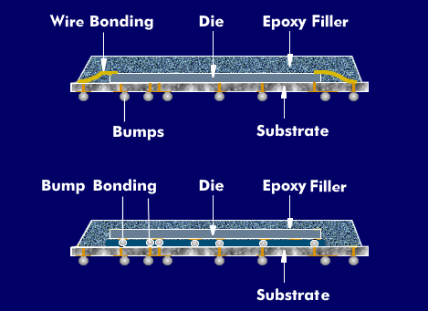
In wire b onding, the contacting areas (pads) on a printed circuit board, a chip and on a substrate are bonded together with extremely thin wires made of gold or aluminum. The chip is attached to the substrate upside down. The pads on the chip are then bonded to the pads on the substrate with an extremely thin wire. The wire-bonding technique is relatively inexpensive. However, it requires relatively large bonding areas.
A further development of wire bonding is the DCA technique, Direct Chip Attach (DCA). In this assembly technique, the package-less chip is placed directly on the substrate or printed circuit board. Chip on Board( CoB) and Chip on Flex( CoF) are among the DCA techniques.
TAB bonding is different. In Tape Automated Bonding (TAB), the chip is first mounted on a prefabricated flexible plastic on which the conductor tracks for the subsequent contacts are also located. Only after placement is the chip contacted at the contacting points.
In bump bonding or chip bonding, the bumps, which are small solder balls placed under the chip, are connected to the substrate. The advantage of this bonding technique is the extremely short connection distances between the chip and the substrate, because this minimizes delay times. The bump bonding technique is used in flip chip technology.
An alternative bonding technique is through-siliconvias( TSV). This technique supports stacked mounting of NAND gates and Dynamic RAMs( DRAM). It is space-saving and offers efficient space utilization of the packages.