conductor path
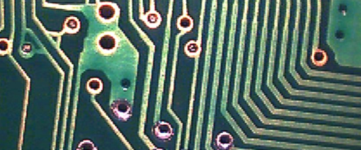
Traces are electrically conductive connections on a printed circuit board. They are used for the current paths, ground and temperature dissipation. To ensure that current is transported with as little loss as possible, the conductor paths are made of copper, which has a low resistivity, and are etched out of the laminated copper coating during PCB manufacture. This is done using lithographic and galvanic processes.
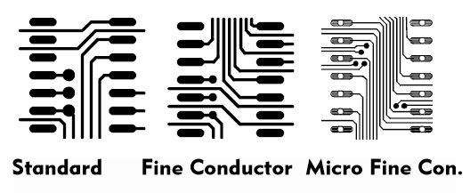
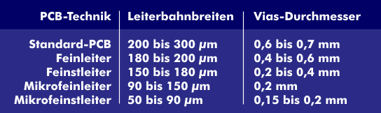
Traces are made in commercially available trace thicknesses. The trace widths, also called traces, are determined by the layout programs and the trace techniques. A distinction is made between standard traces with widths between 300 µm and 200 µm, fine conductors with 180 µm, ultra-fine conductors with 150 µm, and micro-fine and micro-fine conductors with trace structures of 90 µm and 50 µm.
Conductor track thicknesses range from 5 µm to 400 µm without refinement; common conductor track thicknesses are 17.5 µm, 35 µm and 70 µm. The resulting conductor cross-section determines the current-carrying capacity of the trace and thus the current that can flow through it. Traces with smaller cross-sections are used for ultra-fine conductor technology, while thicker ones are used for fine conductor technology and even thicker ones for high-current connections. Traces for high current work with copper inserts, which are placed in milled recesses. These can be located on the top of the PCB or, in the case of multilayer PCBs, between the PCB layers. If wires are used as inserts, this is referred to as wirelaid.
If thicker traces are used, they are called thick copper PCBs. Their track thickness is more than 105 µm. The distance between two traces is determined by the dielectric strength of the insulation and by the mutual capacitive influence.
Printed circuit boards are not only laminated with copper foil on one side, but are designed as multilayer PCBs on two sides and often in multiple layers. The connection between two or more conductive tracks through the PCB by means of holes and plated-through holes, the vias.