printed circuit board (PCB)
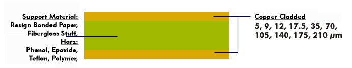
Printed circuit boards are copper-clad, fiberglass-impregnated epoxy resin sheets or polyimide and polyester films on which electronic components are interconnected via conductor tracks. The conductive traces themselves are etched out of the copper lamination using etching techniques. Printed circuit boards use hard paper, glass cloth or cotton paper as the base material, which is reinforced by resins such as phenol, epoxy, Teflon and polymers. This base material is laminated with a copper layer.
For classification purposes, the base materials of printed circuit boards are divided into FR(Flame Retardant) classes. Depending on the carrier material, they are suitable for consumer products, computers, measuring instruments or RF circuits. Frequently used printed circuit boards are flame retardant and have an FR class 4 (FR-4). In addition to rigid PCBs, there are also flexible PCBs, which are used as cable connectors, rigid-flexible PCBs and three-dimensional molded PCBs, among others.
The copper cladding and conductor routing
The simplest version of a printed circuit board is a single-sided standard printed circuit board, which has conductive tracks on one side only. The components are mounted on the top layer. It is called the placement side( BS) or component side. The side with the traces is called the solder side( LS), bottom side or bottom. Since the tracks on the carrier material must always be laid without crossing, it is only possible to work with a single track level for simple electronic circuits. With increasing complexity, printed circuit boards are copper-clad on both sides and must be unbundled with computer programs because of the high degree of complexity. The two sides of the PCB are connected to each other via vias. Both sides of such a bilayer can be equipped with SMD components, integrated circuits, sockets, plugs and connectors.
With the miniaturization of components and the associated lower power consumption, the conductor track structures have also been continuously reduced over the years. While the trace structure of standard PCBs in the 1980s was still between 300 µm and 200 µm, in the following years the trace width was reduced to 180 µm with fine condu ctors and to 150 µm with ultra-fine conductors. In the subsequent technologies with microfine conductors and microfine conductors, the conductor track structures were further reduced to 90 µm and 50 µm.
The copper cladding of the carrier material is extremely thin in all PCB designs and has copper overlays of between 5 µm and 210 µm, with the most common claddings being 17.5 µm, 35 µm and 70 µm. The thin copper overlays are used for ultra-fine conductors, while thicker ones are used for fine conductors and even thicker ones for standard traces and high- current connections. For high currents there is thick copper and wirelaid. Thick copper is used for copper thicknesses of 105 µm and above. The layer thicknesses are 210 µm, 400 µm and in special cases 500 µm. Wirelaid is also an inlay or embedded technology in which high-current conductor tracks are placed between individual PCB layers.
Higher packing density through multilayer technology
If double-sided conductor routing is not sufficient for circuit implementation, the trend is moving to multilayer printed circuit boards. In this process, several thinner epoxy resin boards, all of which have laminated conductor tracks, are bonded to each other with a precise fit using prepregs.
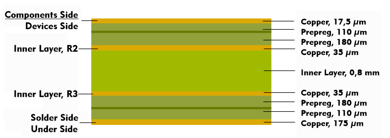
As complexity continues to increase, epoxy resin boards are replaced by copper-clad polyimide or polyester films, which can be as thin as 50 µm. As a result, a printed circuit board can consist of several conductor layers, which can easily be 10 to 20. The limit of multilayer technology is about 48 layers. At this number of layers, the carrier material and the prepregs become extremely thin, which can lead to problems at higher temperatures for lead-free soldering. Contacts between the different traces of multilayer PCBs are provided by vias and vias.
As far as PCB thickness is concerned, Ultra Thin Multilayer( UTM) is a technology for extremely thin multilayer PCBs with thicknesses below 0.5 mm.
Printed circuit boards in HDI technology
To increase the component and track density of standard PCBs, the HDI PCB, High Density Interconnect (HDI), offers a layer structure with smaller track widths and spacing. In the meantime, there are also embedded technologies in which embedded components, which can be active or passive components and also chips, are embedded on the inner layers of multilayer PCBs, thus creating space for active components on the PCB surfaces.
The traces themselves are made of highly conductive material such as copper or silver and are sometimes contacted in gold to limit corrosion. In modern printed circuits, the trace spacing is determined by the contact spacing of the sockets and can be as small as 0.5 mm. Technically, conductor track widths and spacings of 20 micrometers can already be produced. Due to the high degree of fineness, chip-on-boards( CoB) and multi-chip modules( MCM) can be easily integrated into a circuit. The traces themselves can be used to simulate capacitances and high- frequency lines. Examples of this are striplines and microstrips.
The electronic components, sockets, female and male connectors are embedded and plated through the board using through-hole technology( THT), but they can also be soldered, conductive bonded or bonded to the surface of the board using SMT technology.
There are standardized sizes for printed circuit boards. The most commonly used formats for rack-mount insert boards are the euroboard and the double euroboard. Guidelines for PCB manufacturing are issued by the Association Connecting Electronics Industries( IPC).