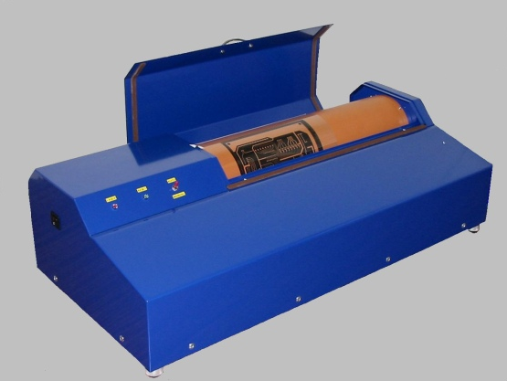
photo plotter
A photoplotter is a special plotter that exposes black and white film material via a light source. The exposed and developed film material forms the basis for the production of printed circuit boards.
The light source is a sharply focused laser beam that is passed over the monochromatic film material in the X and Y directions or in a raster scan, exposing it. The subsequently developed and fixed film material - the photoplot - shows the locations that later form the traces, ground planes, vias, pads and vias on the printed circuit board.
Similar to printed circuit boards, photoplotters are also used to create masks for integrated circuits. However, here the larger photoplots are reduced to photomasks.
As far as the light source for exposing the film material is concerned, over the years green luminous argon-ion lasers and blue luminous helium- cadmium lasers have been used. More recent techniques use red lasers or even light-emitting diodes(LEDs). Recently, laser direct imaging( LDI) has also been used, in which high- power lasers or xenon lamps directly expose the coated circuit board.
Photoplotters support formats in DIN A4 and A3 and larger and are characterized by extremely high resolution. For example, photoplotters can expose the thinnest lines that are less than 5 µm, or 0.005 mm. This corresponds to around 5,000 dpi.