positive intrinsic negative (fiber optics) (PIN)
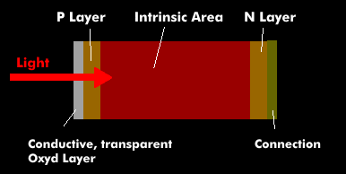
The PIN diode, Positive Intrinsic Negative (PIN), can be an optical detector, i.e. a photodiode, but it can also work as a controllable frequency-dependent resistor or as a power diode; depending on whether it is operated in reverse or forward direction. As a photodiode, the PIN diode operates in the reverse direction and converts light signals into electrical signals.
As can be seen from the name, the PIN diode consists of three layers: a positively doped P layer, a negatively doped N layer, and the intrinsic region located between the two. The intrinsic region is a specific region in which there are only a few free charge carriers. The intrinsic region has a width of about 500 nm to 1,000 nm, whereas the p-layer and the n-layer are only about 10 nm to 30 nm wide. When light falls on the intrinsic region, electrons are torn from the atomic bond and are available for charge transport. The higher the light intensity, the more free electrons are available.
In addition to the PIN diode, the more sensitive APD diodes or phototransistors are also used in E/O converters. The PIN diode is less sensitive than the avalanche photo diode (APD), but is more temperature stable and less expensive. Peak sensitivity values range from -40 dBm (25 Mbit/s) to -55 dB (2 Mbit/s) at 850 nm wavelength.
If the PIN diode is operated in the forward direction, then the space charge zone(RLZ) can be controlled in width, giving it the function of a capacitive resistor. In this function, the PIN diode is used in RF circuits, such as RF attenuators.