thin fine-pitch ball grid array (package) (TFBGA)
The TFBGA package (Thin Fine-Pitch Ball Grid Array) is comparable to the BGA package with the difference that the spherically shaped solder pads on the underside of the package have a smaller spacing. This is only 0.5 mm to 1.0 mm.
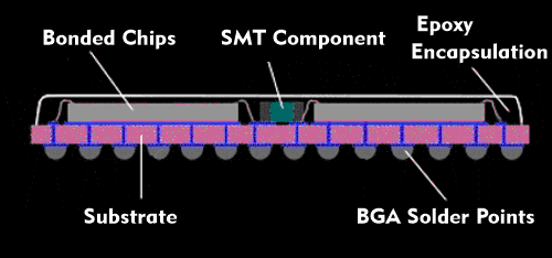
As with the BGA package, the solder pads are arranged as an array in rows and columns. In addition, the TFBGA packages are only 1.2 mm thick. The difference between TFBGA and VFBGA (Very-Thin Fine-Pitch Ball Grid Array) is the thickness of the package, which is only 1.0 mm thick in VFBGA.
The outer dimensions of TFBGA (Thin Fine-Pitch Ball Grid Array) packages are standardized by the Joint Electron Device Engineering Council( JEDEC).