thick film technic (TF)
Thick film technology is a process for manufacturing electronic components and integrated circuits( IC) in microelectronics. It is mainly used in optoelectronics and high- frequency technology for microwave circuits, microwave amplifiers,filters,couplers and oscillators and for microstrips. Thick film technology is based on individual layers of conductive traces, passive and active components stacked on top of each other to form a thick film circuit.
In thick film technology, each individual layer is built on an extremely thin insulator substrate. This can be a thin ceramic plate or a film of temperature-stable low-temperature cofired ceramics( LTCC), it can be glass substrate or aluminum oxide. There are two different thick film manufacturing processes for depositing the conductive tracks and electronic components, the subtractive process and the additive process.
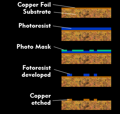
The subtractive process is an etching process, which is also used in the manufacture of printed circuit boards, and in which individual sections are etched out of the substrate laminated over its entire surface with thin copper. For this purpose, the laminated substrate is coated with photoresist and provided with a photomask. After subsequent exposure to UV light, the photoresist is developed wherever it was exposed. Only the unexposed areas remain and the complete copper lamination. This is etched away in the areas that are not protected by the photoresist. Afterwards, the remaining photoresist is removed and the conductive tracks remain on the substrate.
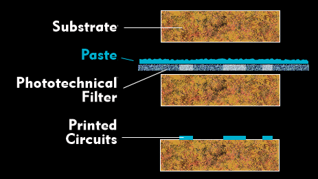
The manufacturing process is different for the additive process, in which the individual layers are created using screen printing. In this technology, pastes made of various more or less strongly conductive or also non-conductive materials are pressed through the photo-structured screen at the points where the screen has been photo-prepared. The individual layers have different recesses and coatings and are printed sequentially. After sintering, they have the desired electrical properties. Several layers, each of which is printed several times, stacked on top of each other form the thick-film circuit.
The pastes for the conductive tracks are pastes with copper, silver or gold-platinum. Resistor pastes, on the other hand, consist of metal oxides and mixtures of metals and metal oxides, and insulating pastes of polymers. The layer thicknesses are between 10 µm and 50 µm. Active components such as diodes and transistors are later applied to the thick-film circuit.