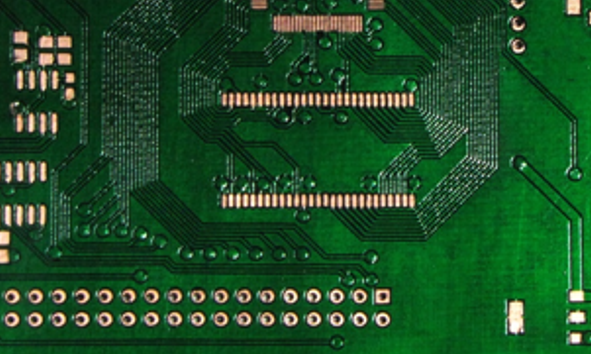
solder stop mask
During PCB manufacture, the conductor tracks are protected against etchants and corrosion with a solder resist. The solder resist also prevents unwanted solder bridges (jumpers) from forming between closely spaced traces or solder pads. For these reasons, a mask of peel-off lacquer is applied before reflow or wave soldering. Such masking is also called resist, photoresist, etch resist, metal resist, dry film resist or galvanoresist.
Photoresist is a laminated, cast or printed photosensitive resist exposed with laser exposure, Laser Direct Imaging( LDI). The exposed/unexposed areas can then be removed as positive resists or negative resists with a developer. Etch resists are film resists that protect the copper lamination from the etching liquid. This can be a tin layer.
Solder resist masks are applied to the printed circuit boards using a photolithographic process or screen printing. In the resist, the soldering points for the components are recessed. In automatic PCB production, the solder resist masks form another layer in the calculation of the various PCB levels and are output by the CAD systems in Gerber format. In addition to the printed solder resist masks, there are also peel-off solder resist masks which serve to protect gold contacts and are removed after the soldering process.