semiconductor
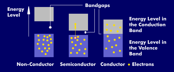
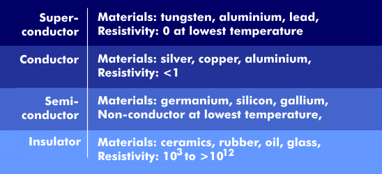
Inelectronics, a distinction is made between materials that conduct electricity, the conductors, and others that do not conduct electricity, the non-conductors (insulator), and still others that are to be classified between conductor and non-conductor because of their crystalline structure, the semiconductors.
The conductivity of condu ctors, semiconductors and non-conductors is given by the band gap between the conduction band and the valence band. While conductors have no band gap, in semiconductors it is between 0.4 electron volts( eV) and 3.6 eV. For non-conductors, it is much higher.
Chemical elements with semiconductor properties
Semiconductors include the chemical elements boron, sulfur, selenium( Se) and tellurium. In microelectronics, mainly germanium( Ge) and silicon( Si) are used as elemental semiconductors, semiconductors consisting of only one chemical element. In addition, there is the large group of compound semiconductors, which includes silicon germanium( SiGe), silicon carbide( SiC), gallium arsenide ( GaAs), gallium nitride( GaN), indium phosphide( InP) and also carbon compounds, from which organic semiconductors are made.
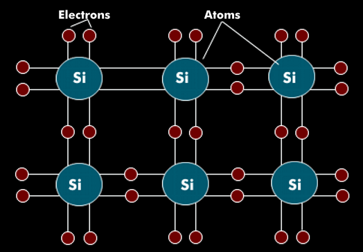
In semiconductors, few or no free electrons are available for current transport. At 0 Kelvin, a semiconductor has the properties of an insulator because there are no electrons in the conduction band. In the case of silicon, which has 14 electrons in three electron shells, the valence band has 4 electrons. In pure silicon, these are paired with four valence electrons of each of the neighboring atoms, so that no free electron is available for current transport.
The energy transport in semiconductors
With increased energy supply through heat or light, the electrons in the valence bands can detach and take over current transport as free electrons in the conduction band. As a result, the semiconductor becomes more conductive and its properties are comparable to those of a conductor. If a bound electron detaches from the bond, it leaves an electron gap in the valence shell, which is called a hole. The transport of current in a semiconductor therefore takes place in two ways: the transport of electrons and the transport of holes, or missing electrons.
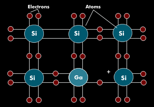
By selective impurity, the doping, of the semiconductor material, for example with arsenic(As), which has five valence electrons, the semiconductor material obtains an electron surplus, it is therefore called N-material. Semiconductor components such as diodes, transistors, thyristors, etc. always consist of two or more N and P layers in which the current flow can be controlled by applying supply and/or control voltages.