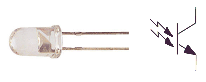
photo transistor
Like the photodiode, the phototransistor is based on the photoelectric effect. This effect causes the properties of a semiconductor path to change when light strikes it due to the impact of photons. This is the collector-base junction, which acts as a photodiode and generates the base current for the phototransistor. This is amplified by the current amplification of the transistor.
As a result, the phototransistor has a much higher sensitivity compared to the photodiode. However, the inertia is higher than that of the photodiode, which means that the phototransistor can only be used in applications with a low pulse frequency. The rise times of the phototransistor are between 1 µs and 100 µs, depending on the load resistance.
The spectral sensitivity is comparable to that of the photodiode, i.e., phototransistors made of germanium have their maximum at about 1,500 nm, those made of silicon at about 800 nm. Both wavelengths are in the infrared range and thus above the visible wavelengths. The sensitivity curve depends on the material of the transistor package. A transparent package has a broader sensitivity curve than a black epoxy package. The maximum sensitivity is for infrared in the wavelength range at approx. 850 nm.