memory chip
With the development of the semiconductor, the technological prerequisites for semiconductor-based data storage were in place. In 1968, the first semiconductor memory, a MOS-based random access memory( RAM) in LSI technology, Large Scale Integration (LSI), was introduced with a clock rate of 4.77 MHz.
With the technological advancement of LSI technology to Very Large Scale Integration( VLSI) and Ultra Large Scale Integration( ULSI), new high- performance memory chips were developed, dramatically increasing memory capacity, data transfer rate and clock speed. The latter reaches values of 800 MHz in modern memory chips.
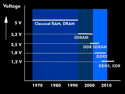
In order to increase the data transfer rates of memory chips, processes were developed in which several data transfers are executed in one clock period. This is the case with DDR technology, in which the rising and falling edges of the clock signal are used for the data transfer. In other processes such as the QBM process, Quad Band Memory (QBM), the data transfer even takes place at four different times of the clock signal. The architecture of the memory bus has also been further developed for higher transfer rates. The Rambus architecture and the Fully Buffered DIMM( FB-DIMM) should be mentioned here. Furthermore, it can be seen that the supply voltage has been constantly reduced. The reason for this is the power dissipation of the memory chips, which increases quadratically with the supply voltage.
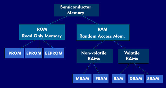
These developments gave rise to many powerful variants of classic RAM, such as Dynamic Random Access Memory( DRAM), Fast Page Mode DRAM ( FPM-DRAM), Magneto-Resistive RAM( MRAM), Extended Data Output DRAM ( EDO-DRAM), Synchronous DRAM ( SDRAM), Synchronous Link DRAM ( SLDRAM), Double Date Rate Synchronous DRAM ( DDR-SDRAM), Enhanced Dynamic Random Access Memory (EDRAM) and Extreme Data Rate DRAM( XDR-DRAM).