fine line metal (FLM)
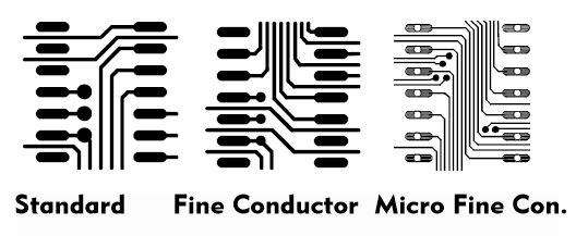
The miniaturization of electronic components and chips has inevitably led to more compact printed circuit boards with reduced conductor structures. These techniques, which were developed in the 1990s and have led to the HDI circuit board, among other things, distinguish in their conductor structures between fine conductors, ultra-fine conductors, micro-fine conductors and micro-fine conductors.
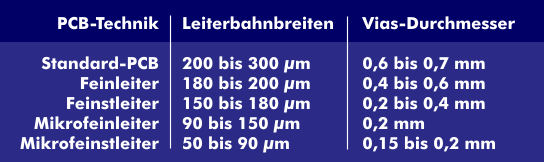
The fine conductor technologies differ in the structure of their conductor paths, the size of the pads, vias and microvias. If standard conductor paths have a conductor path structure between 300 µm and 200 µm, that of the fine conductor technology is 180 µm, of the ultrafine conductor technology 150 µm, of the microfine conductor and microfine conductor technology 90 µm and 50 µm.
The same applies to the vias, which are 0.60 mm in size for standard PCBs, only 0.40 mm for fine conductors and only 0.20 mm and 0.15 mm for ultrafine and microfine conductors.
The fine-conductor technology is used, among other things, in SMT technology, that of ultra-fine conductors in fine- pitch technology, and that of micro-fine conductors and micro-fine conductors in chip-on-board( CoB) and multi-chip modules( MCM).