chip manufacturing
The production of chips consists of many individual steps, starting with the growth of a silicon cylinder, the ingots, continuing with the production of the wafers and the lithographic exposure of the integrated circuits, passing through several tests and ending with the encapsulation of the chips in packages.
Silicon rods or cylinders: The starting material for chip fabrication is a grown semiconductor cylinder made of silicon or another semiconductor material.
-aus-monokristallinem-Silizium-Foto-http-de-yixinwafer-com.png)
These silicon rods or cylinders are called ingots and can be made of high-purity monocrystalline or polycrystalline silicon doped with various chemical elements such as boron (B), phosphorus (P), arsenic ( As) and antimony (Sb). The diameters of the silicon cylinders range from 50 mm to 450 mm, and their lengths from 50 cm to 1 m.
Wafers: The ingots are cut into extremely thin slices by laser technology. The thickness can be only a few hundred micrometers. The wafer surfaces are cleaned in several cleaning and polishing processes, freed from scratches and polished several times in the clean room. They then undergo a final cleaning and an exact inspection of the wafer surface. Before the wafer surface can be lithographically processed, a photoresist, the resist, is applied to the surface.
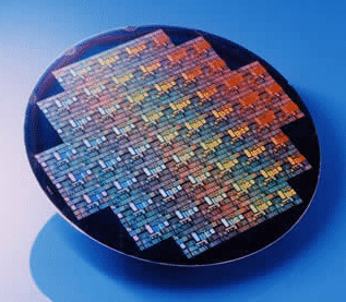
Lithographic processing: In lithographic processing, the photomasks with the chip structures are extremely reduced in size via lens systems and projected onto the wafer. UV light is used for this projection because it has shorter wavelengths than daylight and thus achieves a higher resolution. DUV lithography and EUV lithography are used as projection methods, with which the chip structures are burned into the resist. Subsequently, the structures burned into the photoresist are developed by etching and heating.
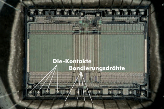
Preparation of the exposed chips: After the chip structures are exposed, the photoresist is removed. This completes a wafer processing cycle for a single chip layer. The other chip layers are processed accordingly and wired by means of bonding. Once all required cycles are completed, the chip cores are cut out of the wafer using dicing and tested. Finally, the chips are encapsulated in a special package using packaging.